


Today we’d like to introduce you to Songyun Gu.
Hi Songyun, so excited to have you with us today. What can you tell us about your story?
I have been working on optical science and nanotechnology for many years. My journey began in 2015. Back then, it was not a super popular choice to study optical science (many of my fellow college mates went for computer science). But I like the magic of optics, not only because it pushes forward the fundamental physics but also because of its potential to be applied in many consumer electronics to benefit our daily lives. As a result, I pursued my bachelor’s degree in optical science and engineering at Zhejiang University, a top-notch University in China. I am also happy to be a part of the Mixed Class of Chu Kochen Honors College, where a group of distinguished undergraduates are assembled. Many of my characteristics, like perfectionism, criticism, and pragmatism, grown at that time during the interaction with my peers. I was also selected to be a member of the University Innovation Fellows launched by Stanford University.
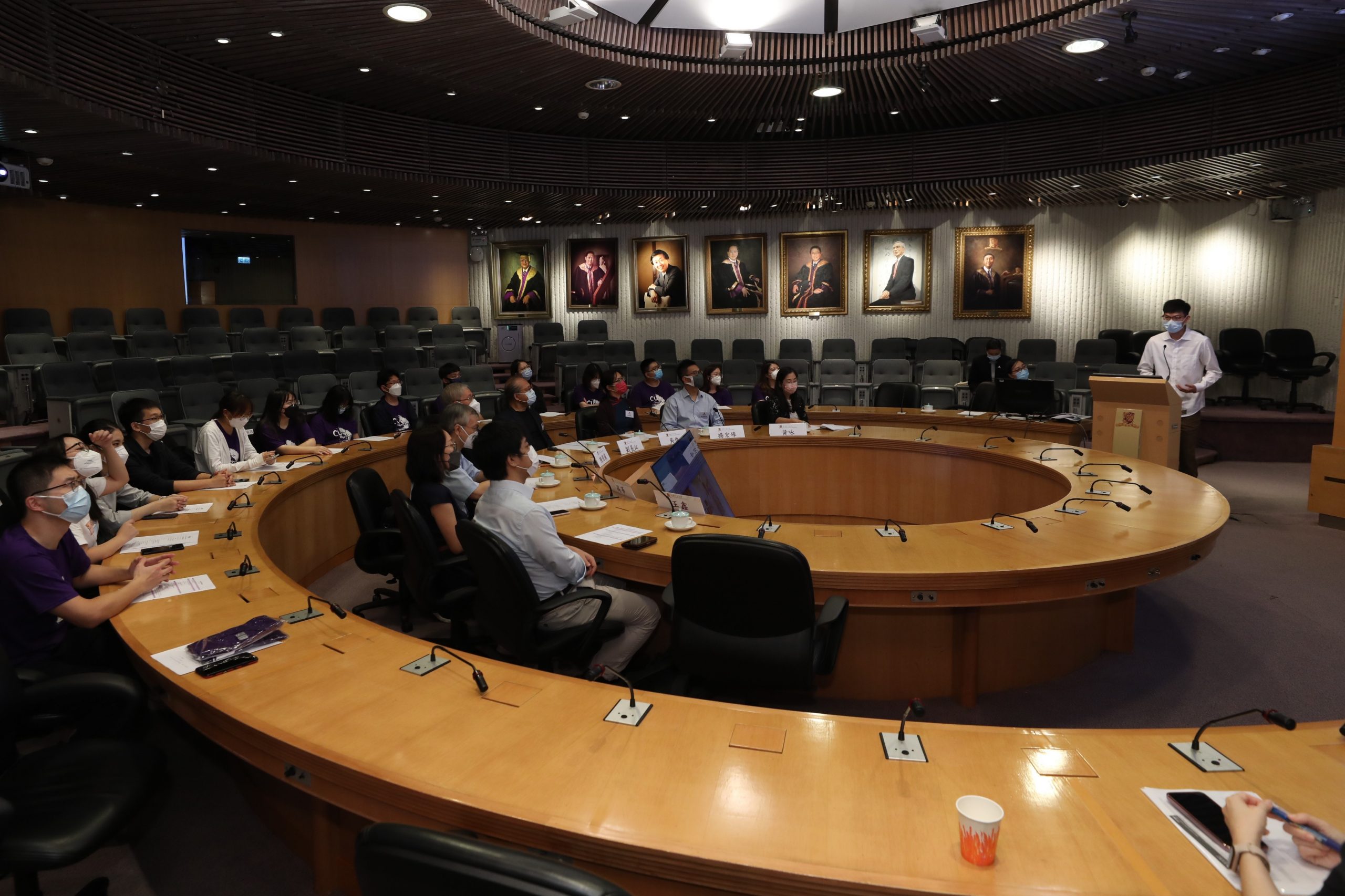
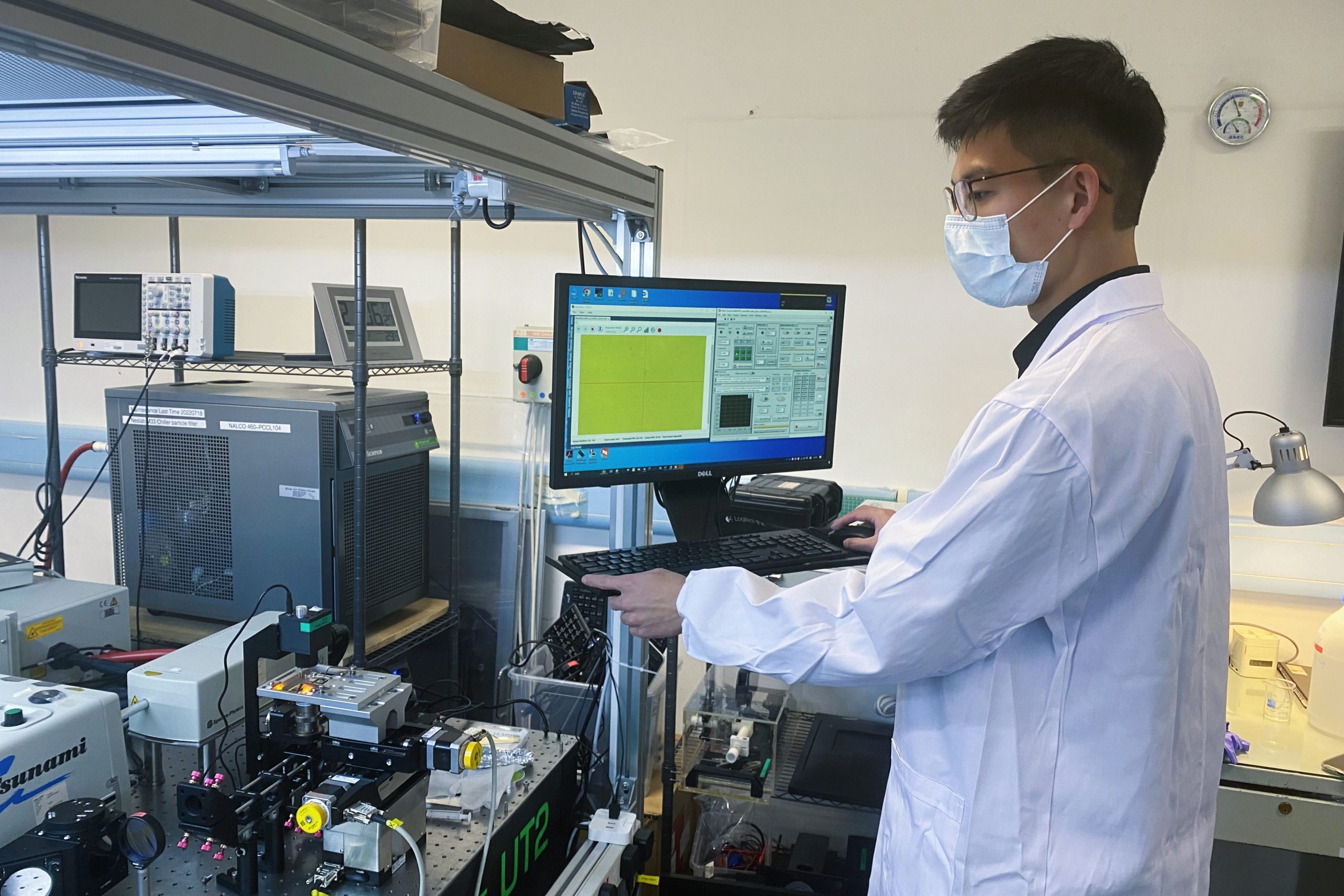
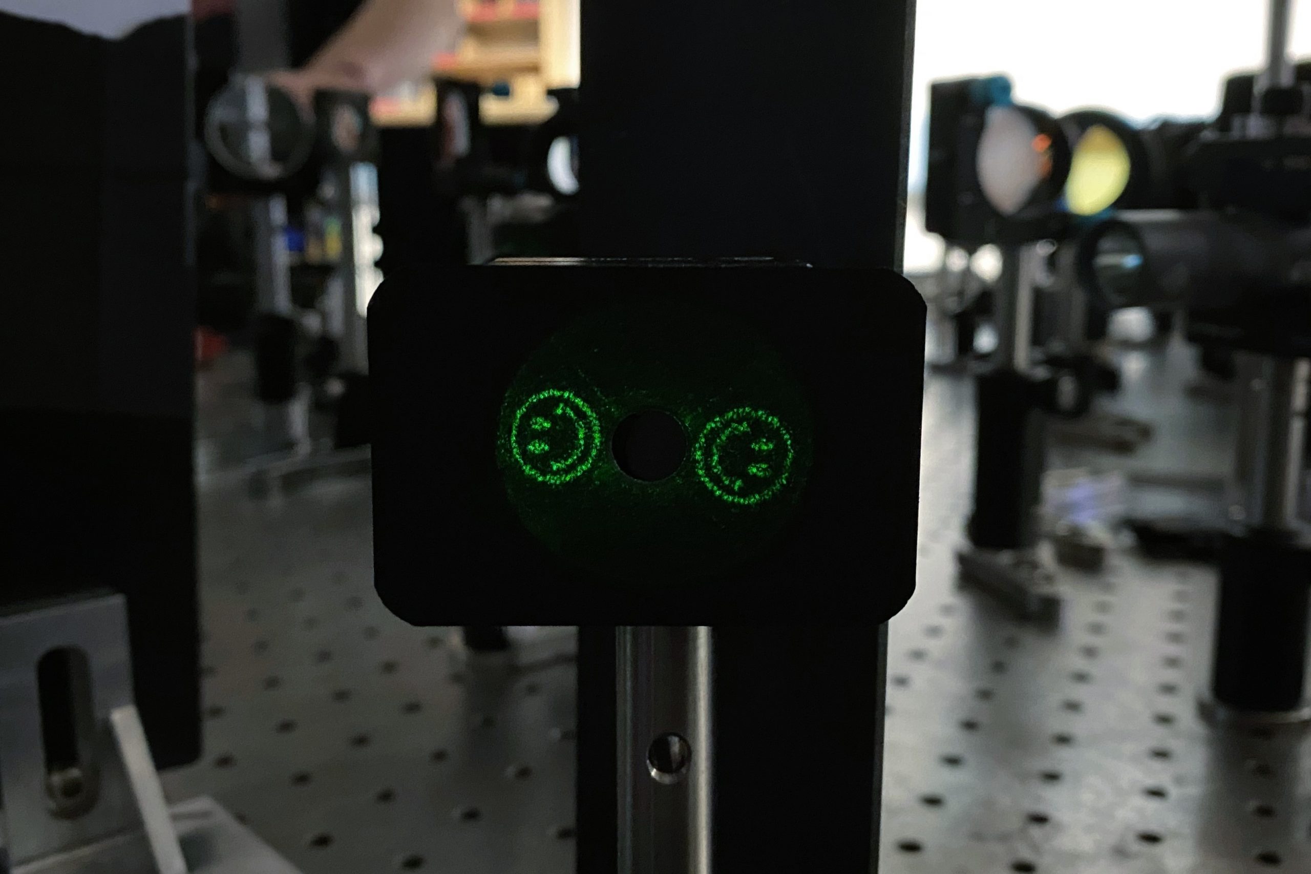
I went to Hong Kong (Prof. Shih-Chi Chen’s Group at The Chinese University of Hong Kong) later in 2019 to pursue my PhD degree in precision engineering, where I started my work on developing new nanofabrication technologies. During that time, I met many people that are of great importance to me, including Prof. Chen, Prof. Fei Han, and a series of names that I acknowledged in my Ph.D. thesis. With their help and the hard work, I developed a new 3D nanofabrication technology that breaks every record compared with current technologies. Most of the research process are painful. But it is rewarding to finally see our work gets published on Science Magazine and gets a series of awards, including the 10 Major Breakthroughs in Optics (China), Silver Medal of Geneva International Exhibition of Inventions, etc. This technology is not under commercialization by Astra Optics Limited and will continuously generate impact for nanoscience and engineering.
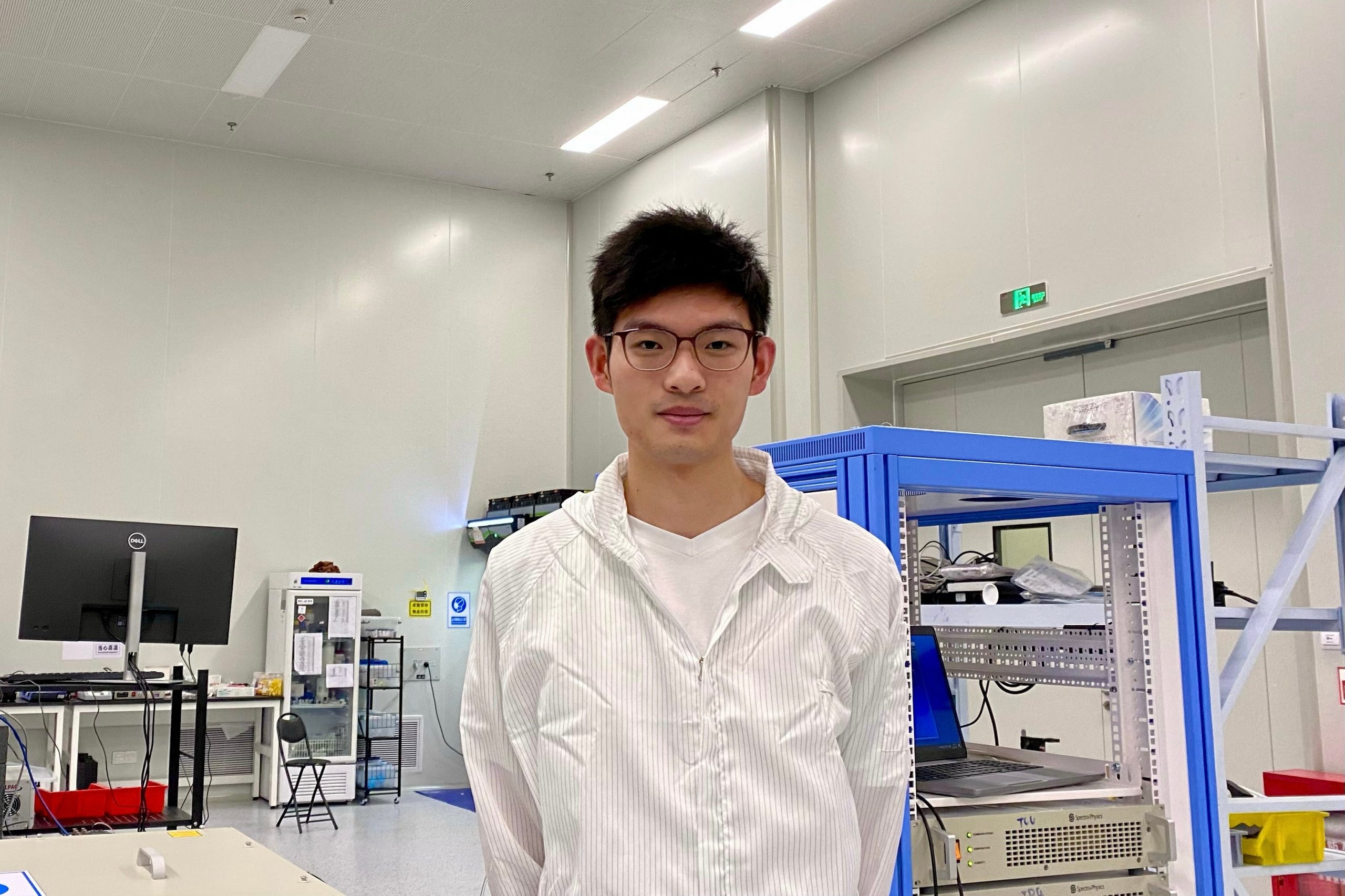
After obtaining my PhD degree, I decided to continue to do research on nanotechnology and nanofabrication at Lawrence Livermore National Lab, where many big science breakthroughs are ongoing. It is really exciting to work here. I can’t tell more details about my current work. But I believe it will be something that can generate a wider impact to humanity. I am proud of my choice and will remain committed to pushing the boundaries of what is possible.
Would you say it’s been a smooth road, and if not, what are some of the biggest challenges you’ve faced along the way?
Doing scientific research surely is not something like cooking based on a recipe. I face questions that may or may not have answers every day. I can recall some of the detailed struggles along the way.
It is specially challenging to handle nanostructures. It cannot be touched by hand of course. And any operations could lead to the disappearance of the tiny delicate structures during laboratory prototyping.
Unable to see the ultrafast optical process is another factor that could drive me crazy. Imagine you couldn’t see the dish you are cooking right now. I also cannot see what I am doing during the optical process.
Sometimes it is the small things that can be in the way, like a tiny piece of dust floating on top of the fabricated nanostructure. And sometimes, it is more challenging stuff like modeling the dynamic photochemical process. But in the end, my PhD journey teaches me how to deal with these struggles. Some can be cleverly mitigated, some can be solved with patience, and some can be addressed by consulting people of knowledge.
Thanks – so, what else should our readers know about your work and what you’re currently focused on?
I am a researcher on nanotechnology. And I am known for the invention of a new hydrogel-based 3D nanofabrication technology, which revolutionize the way 3D nanostructures of different materials are generated.
This technology is more than just a technical achievement; it’s a gateway to endless possibilities. We’re talking about the precise patterning of materials at the nanoscale, which paves the way for advanced optics, electronics, custom medical devices, and entirely new materials with unprecedented properties and functionalities. The implications for fields like nanoelectronics, biosensors, and even the realm of nanorobots are profound, hinting at a future where science fiction becomes our everyday reality. More than the technical metrics, what excites me most is the potential of our work to inspire and enable further innovation across a broad spectrum of fields and industries.
As for my uniqueness, unlike traditional paths that might focus solely on one aspect of science or technology, I’ve built my career at the intersection of multiple disciplines—combining optical science, nano-chemistry, and precision engineering. This holistic perspective enables me to see beyond conventional boundaries and develop innovative solutions that others might overlook.
Let’s talk about our city – what do you love? What do you not love?
I like the diversity of Los Angeles. Many good university and research institutes make LA a great city for innovation. There are many museum about art, technology, and science in LA, where I really like to spend my weekend. I am really happy for the kids that grow up in this great city who can feel this creative culture since childhood.
I don’t like the traffic and the smell of the underground.